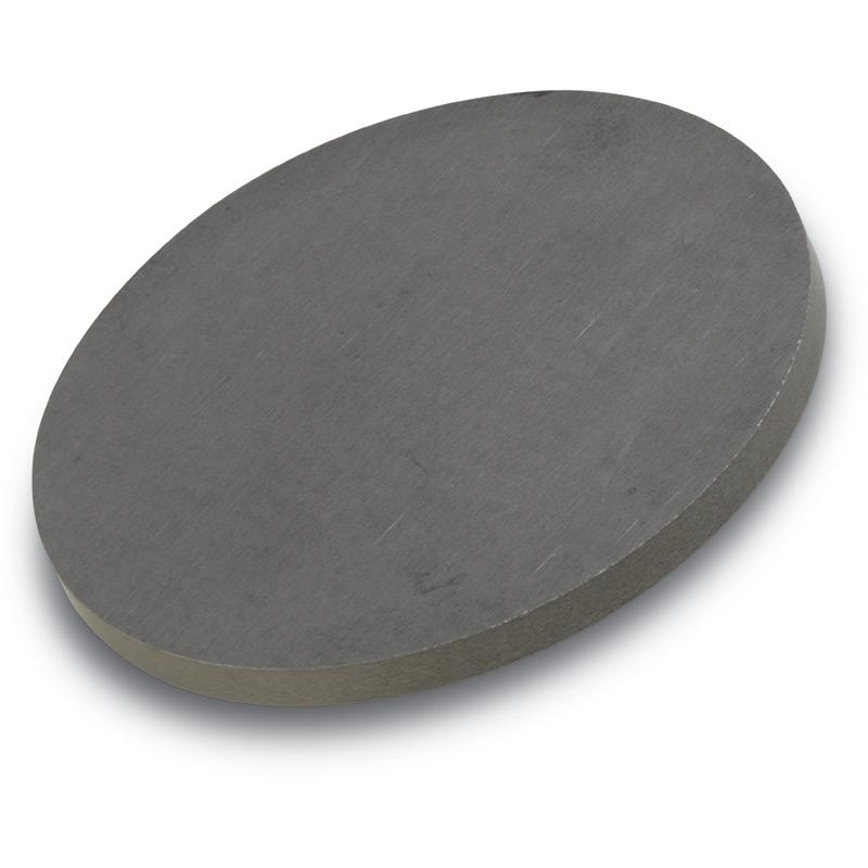
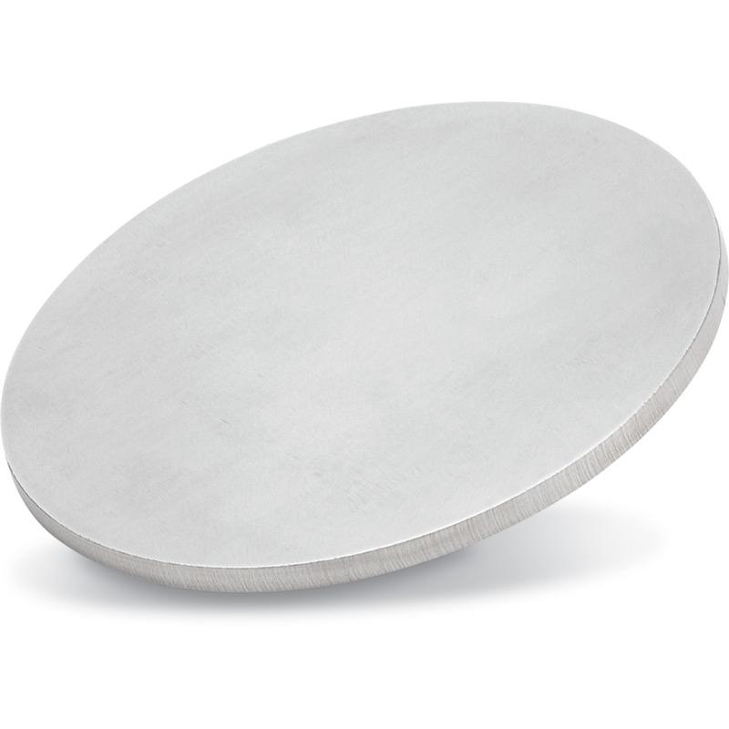
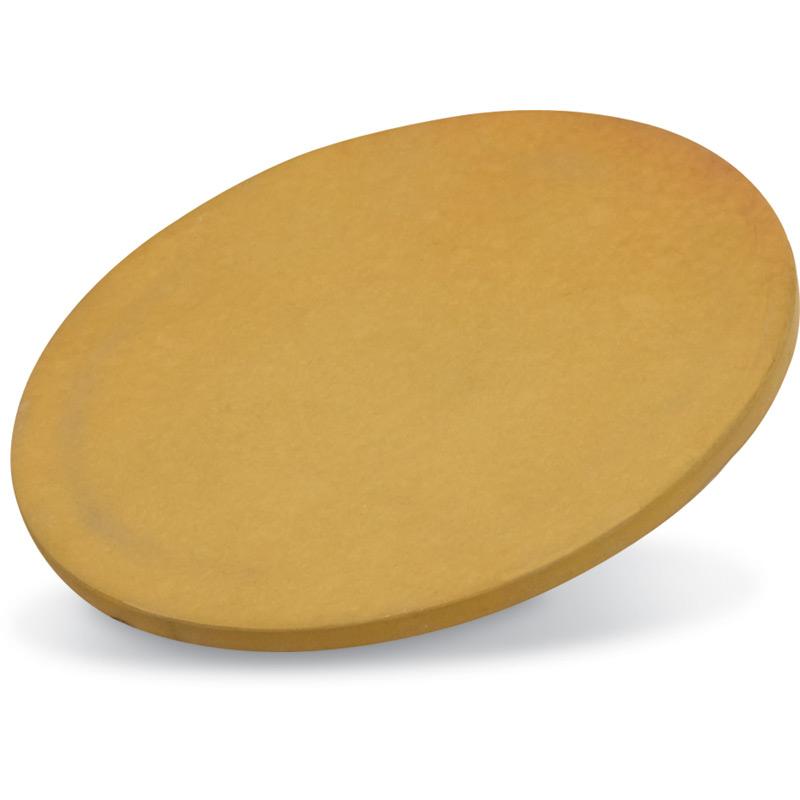
High-purity Tantalum Nitride (TaN) sputtering targets for DC/RF deposition of ultra-thin Cu diffusion barrier layers in advanced CMOS and 3D IC interconnect technology. TaN is the industry-standard diffusion barrier between low-k dielectric and Cu interconnects at the 28 nm node and below, offering exceptional barrier properties, low electrical resistivity (~200–300 µΩ·cm), and excellent adhesion to both Cu seed layers and SiO₂/low-k dielectrics.
Specifications
| Parameter | Value / Details |
|---|
| Material | Tantalum Nitride (TaN) |
| Purity | 99.5% (2N5) / 99.9% (3N) |
| Electrical Resistivity | ~200–300 µΩ·cm (film — diffusion barrier range) |
| Crystal Structure | Hexagonal (ε-TaN) / cubic (δ-TaN) — process dependent |
| Relative Density | > 95% theoretical density |
| Standard Sizes | Ø 50.8 mm × 3 mm / Ø 76.2 mm × 3 mm (disc) — custom sizes available |
| Sputtering Method | DC magnetron — compound target or reactive Ta + N₂ |
| Process Gas | Ar / Ar + N₂ (N₂ % controls phase: Ta, Ta₂N, TaN, Ta₃N₅) |
| Film Applications | Cu diffusion barrier, IC interconnect, MEMS, ferroelectric devices |
| Packaging | Vacuum-sealed bag + foam-padded box — ICP-OES purity certificate included |
| Bonding | Cu or In backing plate bonding available on request |
| Storage | Cool, dry — stable in air |
| Lead Time | 3–7 days (stock) / 10–20 days (custom) |
| Customization | TaN-Ta bilayer targets, custom N content, size on request |
Trade Information
| Trade Detail | Information |
|---|
| Minimum Order Quantity | 1 Piece |
| Supply Ability | 100 Pieces Per Month |
| Delivery Time | 1–3 Weeks |
| Main Domestic Market | China |
| Export Markets | Worldwide |
| Payment Terms | T/T, L/C, Western Union, PayPal |
| Packaging | Vacuum-sealed bag + foam-padded box |
| Certification | ISO 9001 — purity certificate (ICP-OES) provided |
| Storage | Cool, dry environment — reseal after use |
| Customization | Custom size, purity, shape, bonding, and alloy available |