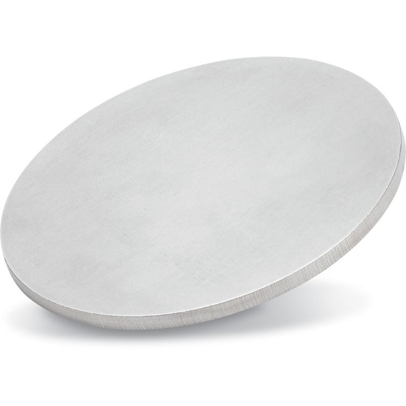
High-purity Tungsten (W) metal sputtering targets for DC magnetron deposition of pure W films, tungsten nitride (W₂N) diffusion barriers, and tungsten silicide (WSi₂) gate electrodes in semiconductor devices. Tungsten has the highest melting point of all metals (3422°C), excellent electrical conductivity, and outstanding thermal stability — making W thin films the material of choice for semiconductor interconnect barriers, X-ray mirrors, and MEMS structural layers.
Specifications
| Parameter | Value / Details |
|---|
| Material | Tungsten (W) — pure metal |
| Purity | 99.95% (3N5) / 99.99% (4N) |
| Melting Point | 3422 °C — highest of all metals |
| Electrical Resistivity | 5.3 µΩ·cm (bulk) |
| Standard Sizes | Ø 50.8 mm × 3 mm / Ø 76.2 mm × 3 mm (disc) — custom sizes available |
| Custom Sizes | Rectangular, plate, tube — any dimension |
| Bonding | Cu or In backing plate bonding available on request |
| Sputtering Mode | DC magnetron (W films) / reactive (W₂N, WO₃, WSi₂) |
| Reactive Gases | N₂ for W₂N / O₂ for WO₃ / SiH₄ for WSi₂ |
| Film Applications | IC diffusion barrier, X-ray mirror, MEMS, gate electrode, hard coating |
| Packaging | Vacuum-sealed bag + foam-padded box — ICP-OES purity certificate included |
| Storage | Stable in air — no special precautions required |
| Lead Time | 3–10 days (stock) / 15–25 days (custom) |
| Customization | W-Ti, W-Mo alloy targets available |
Trade Information
| Trade Detail | Information |
|---|
| Minimum Order Quantity | 1 Piece |
| Supply Ability | 100 Pieces Per Month |
| Delivery Time | 1–3 Weeks |
| Main Domestic Market | China |
| Export Markets | Worldwide |
| Payment Terms | T/T, L/C, Western Union, PayPal |
| Packaging | Vacuum-sealed bag + foam-padded box |
| Certification | ISO 9001 — purity certificate (ICP-OES) provided |
| Storage | Cool, dry environment — reseal after use |
| Customization | Custom size, purity, shape, bonding, and alloy available |