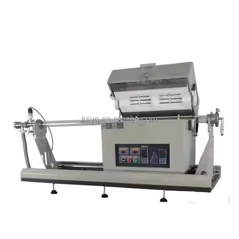
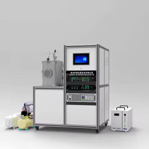
PVD Vacuum Coating Machine — Multi-Material Research and Prototyping
Versatile physical vapour deposition capability — the ability to deposit a wide range of metals, alloys, oxides, and nitrides on diverse substrate types without being constrained to a single deposition method or target material — is the defining requirement for a central thin film deposition facility. This PVD vacuum coating machine is configured to support both DC and RF magnetron sputtering and resistive thermal evaporation in a single large-format stainless steel chamber, with MFC-controlled gas delivery for both inert and reactive deposition processes.
Technical Specifications
| Parameter | Specification |
|---|
| Deposition methods | DC magnetron sputtering, RF magnetron sputtering, resistive thermal evaporation (configurable) |
| Chamber | Stainless steel cylindrical — electropolished interior |
| Target configuration | Up to 2 magnetron sources (DC + RF); thermal evaporation boat positions |
| Target diameter | 2-inch or 3-inch per magnetron source |
| Substrate capacity | Up to Ø 150 mm (6-inch wafer) on motorised rotating carrier |
| Substrate heating | Up to 400 °C optional |
| Ultimate base pressure | ≤ 5 × 10⁻⁶ mbar |
| Pumping system | Turbomolecular (>200 L/s) + rotary vane backing pump |
| Gas delivery | MFC-controlled Ar + two reactive gas lines (O₂, N₂) with upstream isolation valves |
| Control system | Touchscreen PLC with programmable recipe storage — up to 50 process recipes |
| Thickness monitoring | Quartz crystal microbalance (QCM) for real-time deposition rate monitoring |
| Power input | 220 V / 50 Hz — Indian standard; three-phase available for high-power configurations |
| Certifications | CE, ISO compliant |
| Warranty | 12 months from commissioning |
Typical Applications
- Central thin film deposition facility serving multiple research groups
- Optical thin film coating prototyping — anti-reflection, high-reflection stacks
- Hard coating and tribological thin film research — TiN, CrN, DLC
- Semiconductor contact and barrier layer process development
- Transparent electrode development for photovoltaic and display research
- Functional coating development for industrial prototyping applications
This system is specified and configured for each installation. Contact Virospuk with your material range, substrate size, and process requirements — we will design the correct target configuration, gas delivery arrangement, and control system for your facility.